Fabricate your design
Full-wafer runs for your own process and layout, or a slot on our quarterly shared wafer. Al/AlOx/Al junctions, air bridges, flip-chip.
First flip-chip integrated devices delivered October 2025.
FoundryQuantum foundry · Gothenburg and Copenhagen
We fabricate your designs in the Chalmers and DTU cleanrooms, on a schedule you can book, with published performance data for our process.
Designs in. Measured devices out.
256 µs
best measured qubit T1
QiB0, datasheet v2.0, Oct 2025
90–130 µs
average T1, QiB0
datasheet v2.0, Oct 2025
≳1M
resonator Qi at single-photon power
QiB0/QiB2 datasheets
±10%
JJ resistance variation within a block
Q-MPW Technical Guide, Feb 2026
Q-MPW · Q4'26 · Design review
Q4'26 submissions closed 21 Oct. Design review runs until 9 Nov, then fabrication 10 Nov – 11 Dec 2026. Delivery mid-December 2026.
Next round · Q1'27
Q-MPW · Q4'26 · Fabrication
Q4'26 is in fabrication until 11 Dec. Delivery mid-December 2026.
Next round · Q1'27
Q-MPW · Q4'26 · Dicing and shipping
Q4'26 chips are being diced and shipped. Delivery mid-December 2026.
Next round · Q1'27
Q-MPW · Q4'26 · Delivered
Q4'26 chips were delivered mid-December 2026.
Next round · Q1'27
Q-MPW · Q1'27 · Submissions open
33 days left to submit.
Design review 12 Feb – 2 Mar 2027, fabrication 3 Mar – 3 Apr 2027, delivery mid-April 2027.
This round · Q1'27
Q-MPW · Q1'27 · Design review
Q1'27 submissions closed 12 Feb. Design review runs until 2 Mar, then fabrication 3 Mar – 3 Apr 2027. Delivery mid-April 2027.
Next round · Q2'27
Q-MPW · Q1'27 · Fabrication
Q1'27 is in fabrication until 3 Apr. Delivery mid-April 2027.
Next round · Q2'27
Q-MPW · Q1'27 · Dicing and shipping
Q1'27 chips are being diced and shipped. Delivery mid-April 2027.
Next round · Q2'27
Q-MPW · Q2'27 · Submissions open
This round · Q2'27
PDF, 734 kB · Q-MPW Technical & Operational Guide v1.0
Full-wafer runs for your own process and layout, or a slot on our quarterly shared wafer. Al/AlOx/Al junctions, air bridges, flip-chip.
First flip-chip integrated devices delivered October 2025.
FoundryA known-good qubit chip, so you know whether the problem is your chip or your cryostat. Three devices, from four simple qubits to coupled pairs.
Used by Bluefors, QphoX and Kiutra to test their own systems.
Qubit-in-a-BoxReal superconducting qubits in your teaching lab: chip, electronics, fridge, training.
Running in the Niels Bohr Institute's Quantum Training Lab since 2024.
Plug'N'TeachMeasured, not adjectives
We publish what we measure: reference devices, averages, the best result, and the date and datasheet behind each one. If a number isn't in a published, dated source, it isn't on this site.
QiB0 · CS_QIB0_30
Measureddatasheet v2.010 Oct 2025We sign an NDA before you send a single file. Only your team and our foundry see your design. Wafer previews show your chips and nothing else, and design data is handled on a need-to-know basis.
Our quantum devices are EU dual-use items (category 3A001). Every order needs a signed End-User Statement before shipping. Within the EU, and to Australia, Canada, Iceland, Japan, Liechtenstein, New Zealand, Norway, Switzerland, the UK and the US, no individual licence is needed. Anywhere else needs an export licence, which adds time, so tell us your destination early and we'll start the paperwork with you.
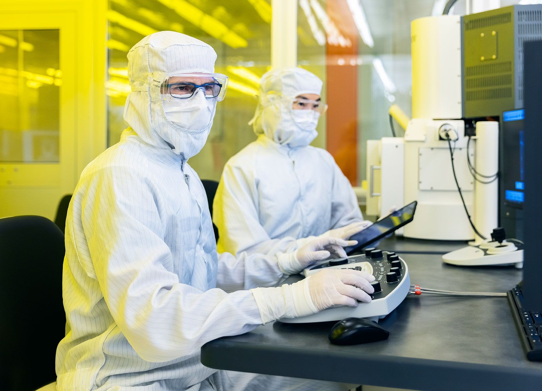
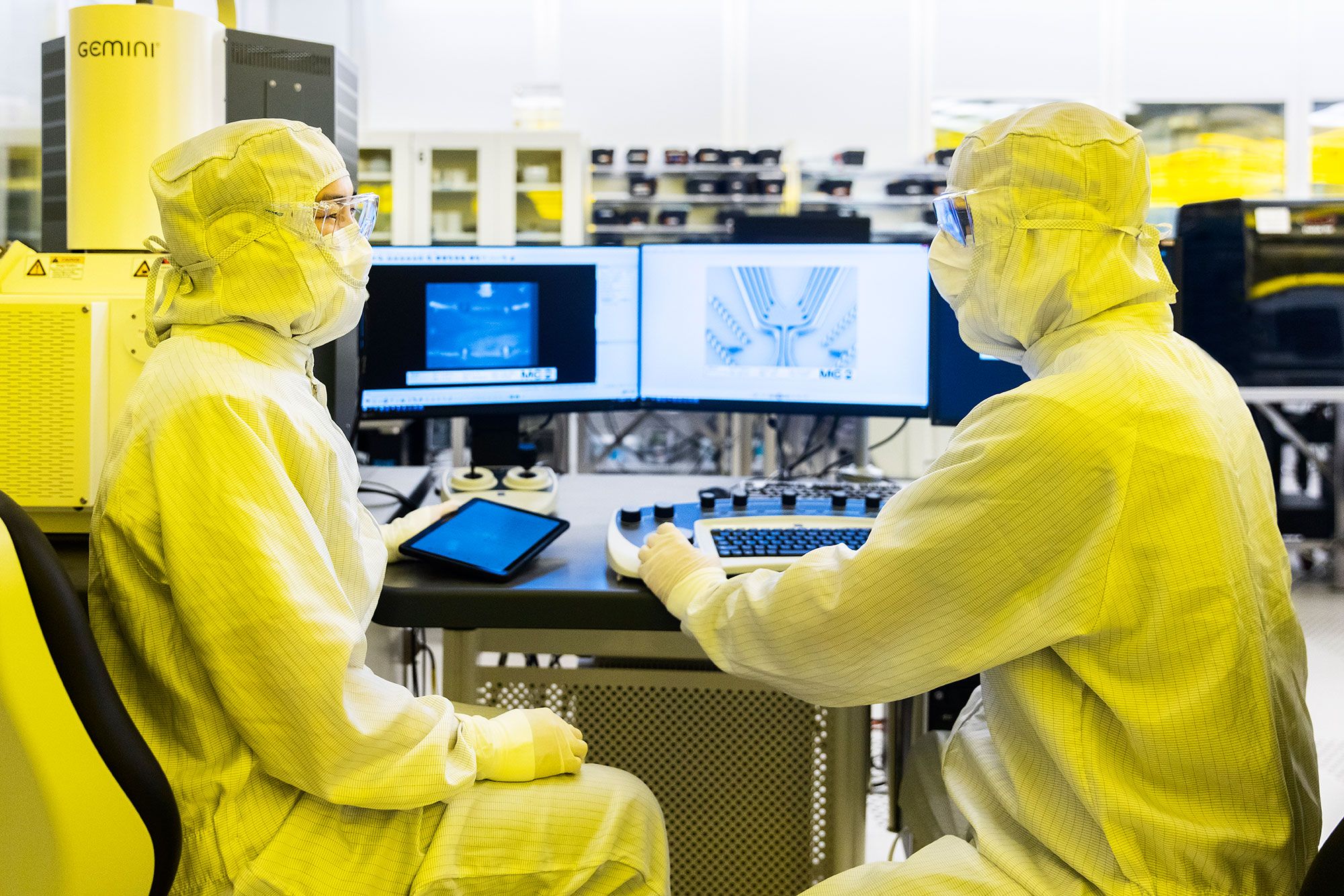
Photos: Francis Löfvenholm
Two cleanrooms, one team
We work in Chalmers MC2 and DTU Nanolab — together more than 10,000 m² of cleanroom and over 2,000 instruments. You get that tooling without paying for our fab. Our Danish team at DTU Science Park works with customers across Denmark and the Nordics.
Who works with us
QiB0 in a paper and an application note on cryogenic measurement setups.
QiB2 in the Quantum Training Lab.
Custom nanofab and microfluidics.
Process development and scale-up.
Also from our cleanroom
Mother-machine molds for cell biology, EBL down to sub-10 nm, membranes, coatings and calibration standards.
People
Many of us came from Chalmers — from its quantum technology lab and from MC2, where one of us made detectors for ESA missions including Herschel and JUICE.
About 15 people · three in four hold a PhD