Nanofab and microfluidics
Hard-to-make structures, since 2012.
Custom nanofabrication for research groups and companies: mother-machine molds, electron-beam lithography down to sub-10 nm, membranes, coatings and calibration standards. Small volumes and complex designs are what we do.
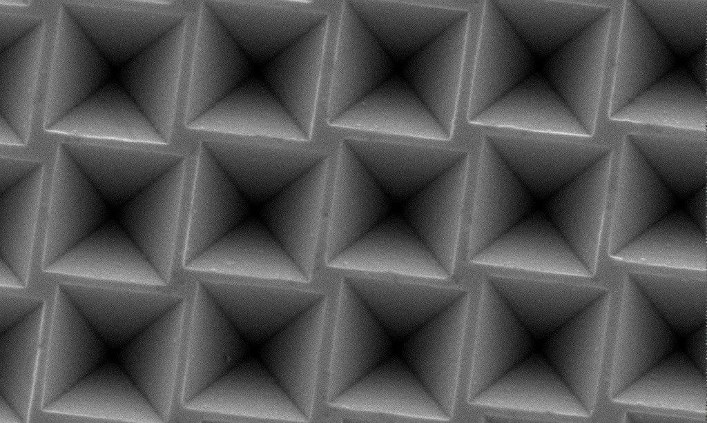
Microfluidics and mother machines
Mother-machine molds and microfluidic chips
Custom molds based on the mother-machine concept, with sub-100 nm features and sub-100 nm overlay between layers. Channel dimensions accurate to under 30 nm, with several channel sizes on one mold. We supply ready-to-use devices, or molds to replicate thousands of devices in your own lab.
For nanofluidics, our FUEC system combines framed chips in glass, fused silica or glass–silicon, chip holders and a pressurising unit.
Used by groups at Uppsala, Harvard, Oxford, Cambridge and UC San Diego
- Feeding channel: fresh medium flows past the channel openings
- Growth channels in several sizes on one mold, dimensions accurate to under 30 nm
- Mother cell, held at the dead end
Mother machine · top view · not to scale
We endorse them. We designed & ordered multiplex mothermachine from them about a year ago. They delivered an excellent product. The price was reasonable, certainly far less than what it cost us back in 2008 at Harvard for the first mothermachine. We will use them again.
Selected papers using our devices
- 2025Tran et al., Nature Communications
- 2017Jones et al., Science
- 2016Kipper et al., ACS Synthetic Biology
- 2014Hammar et al., Nature Genetics
Electron-beam lithography
EBL at the resolution limit, and at wafer scale
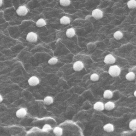
sub-10 nm
Features, transferred into films by lift-off or dry etch
6 nm
Gaps in large-area gold films
8-inch
Wafers for large-area writing (up to)
Used for AR optics, metalenses, diffractive elements, HEMTs, plasmonic sensing, metamaterials and quantum devices.
Devices
Devices to your specification
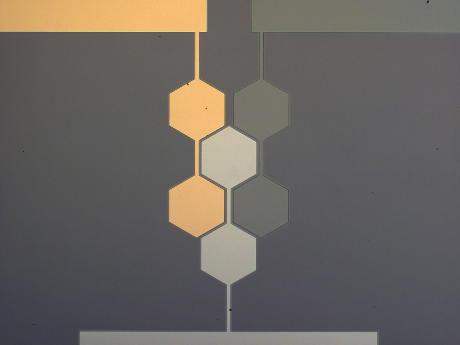
Superconducting nanowire single-photon detectors
For near-infrared and visible light.
Organic field-effect transistors
Sub-20 nm patterning, custom channel geometry, source/drain metallisation, vias for back-gating; bring your own semiconductor or choose with us.
Complex multilayer devices
Many-layer stacks with tight process control.
TEM membranes
Custom materials and dimensions.
…From product design to delivery, ConScience and Joachim have been great at keeping me updated with fabrication and shipment. As for the product itself, they are immaculate, reliable and durable.
OFET references
- 2021Ye et al., Advanced Functional Materials
- 2021Xu et al., Journal of Applied Physics
- 2021Xu et al., Angewandte Chemie International Edition
Coatings
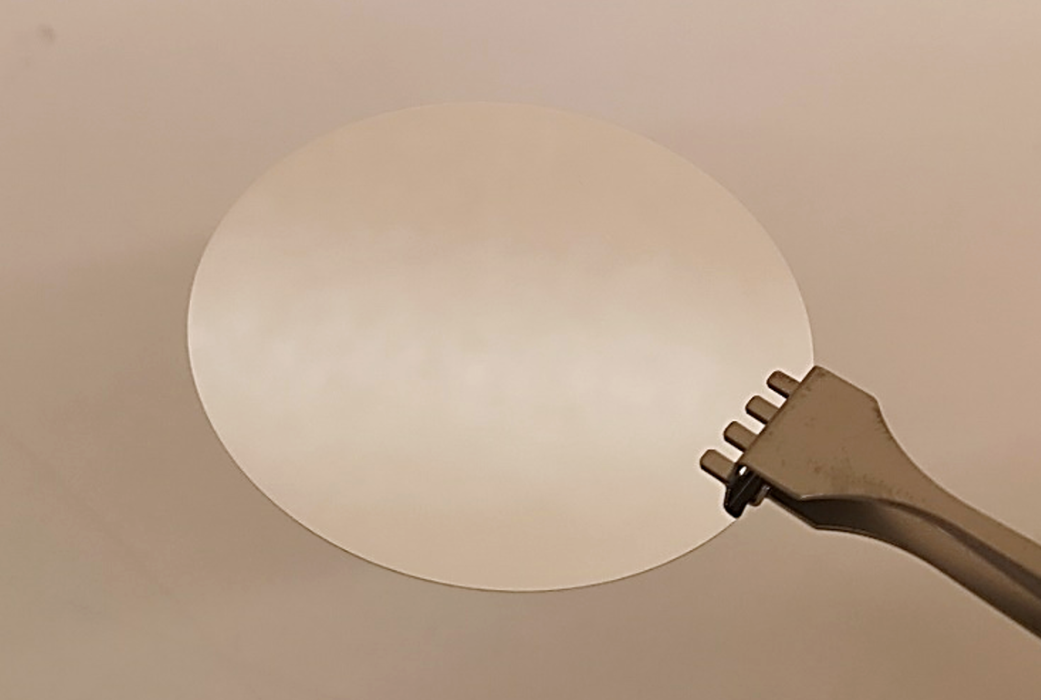
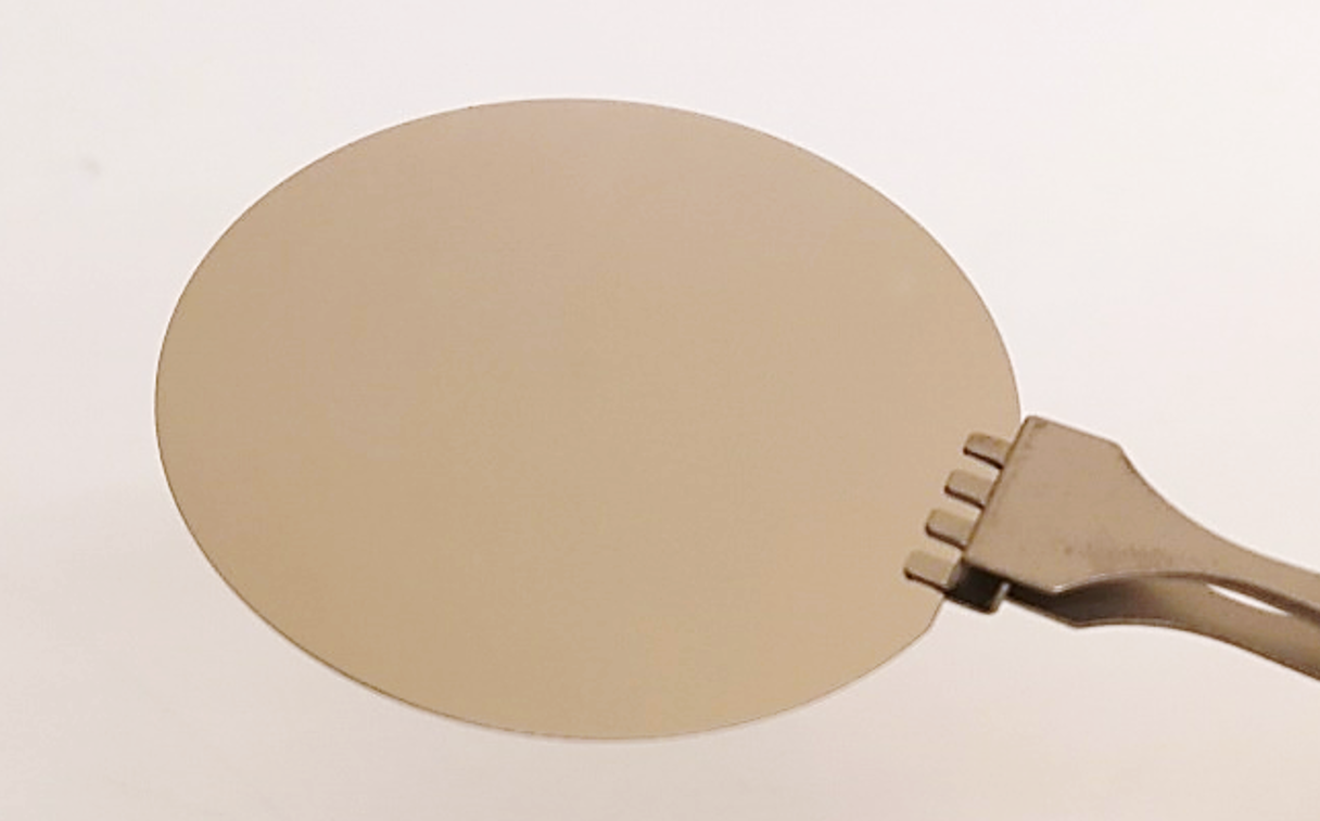
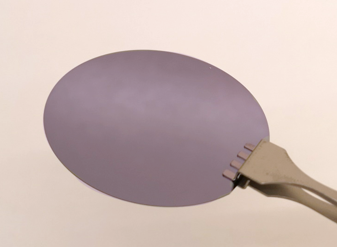
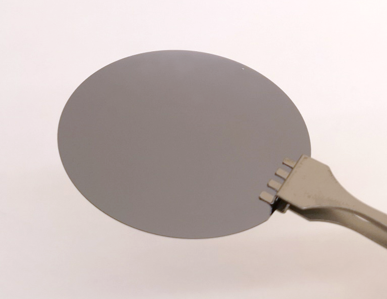
Coated wafers
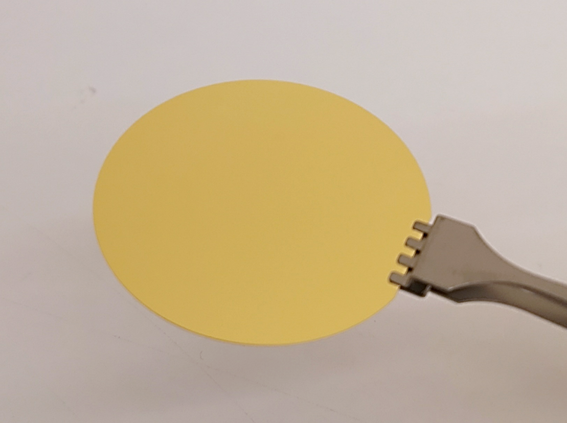
Calibration standards
AFM/KPFM calibration standard
Three work-function metals (Au, Pt, Cr) in a range of patterns and scan directions, validated with the Danish National Metrology Institute (DFM). Custom designs and packaging available.
Developed with support from Vinnova (2019-03545) and Eurostars (E!113474).
Short form
Case studies
The full stories are on the Evidence page.
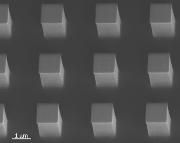
Insplorion
Scaled up nanoplasmonic sensor fabrication with faster throughput and standardised QC.
Read the case study: InsplorionICMAB-CSIC
Reproducible nanostructure masters for soft nanoimprint lithography.
Read the case study: ICMAB-CSICNewcastle University
Nanopillar wafers for the VerCINI vertical-imaging method, made available to other labs.
Read the case study: Newcastle UniversityUC San Diego
Custom mother-machine molds; repeat customer.
Read the case study: UC San Diego
Send us a drawing.
Small volumes and complex designs are what we do.